 | –≠–ª–µ–∫—Ç—Ä–æ–Ω–Ω—ã–π –∫–æ–º–ø–æ–Ω–µ–Ω—Ç: ST485EXDR | –°–∫–∞—á–∞—Ç—å:  PDF PDF  ZIP ZIP |
1/13
September 2003
s
LOW QUIESCENT CURRENT: 300
µ
A
s
DESIGNED FOR RS-485 INTERFACE
APPLICATIONS
s
-7V TO 12V COMMON MODE INPUT
VOLTAGE RANGE
s
DRIVER MAINTAINS HIGH IMPEDANCE IN
3-STATE OR WITH THE POWER OFF
s
70mV TYPICAL INPUT HYSTERESIS
s
30ns PROPAGATION DELAYS, 5ns SKEW
s
OPERATE FROM A SINGLE 5V SUPPLY
s
CURRENT LIMITING AND THERMAL
SHUTDOWN FOR DRIVER OVERLOAD
PROTECTION
s
ESD PROTECTION:
±
15KV (H.B.M.)
±
8KV (IEC-1000-4-2 CONTACT
DISCHARGE)
s
ALLOWS UP TO 64 TRANSCEIVERS ON
THE BUS
DESCRIPTION
The ST485E is al low power transceiver for
RS-485 and RS-422 communication. Each driver
output and receiver input is protected against
±
15KV electrostatic discharge (H.B.M.) (ESD)
shocks, without latcup. These parts contain one
driver
and
one
receiver
in
half
duplex
configuration.
This transceiver draw 300
µ
A (typ.) of supply
current when unloaded or fully loaded with
disabled drivers.
It operates from a single 5V supply.
Driver is short-circuit current limited and is
protected against excessive power dissipation by
thermal shutdown circuitry that place the driver
outputs into a high-impedance state.
The ST485E is designed for bi-directional data
communications on multipoint bus transmission
line (half-duplex applications).
ORDERING CODES
Type
Temperature
Range
Package
Comments
ST485ECN
0 to 70 ∞C
DIP-8
50parts per tube / 40tube per box
ST485EBN
-40 to 85 ∞C
DIP-8
50parts per tube / 40tube per box
ST485EXN
-55 to 125 ∞C
DIP-8
50parts per tube / 40tube per box
ST485ECD
0 to 70 ∞C
SO-8 (Tube)
100parts per tube / 20tube per box
ST485EBD
-40 to 85 ∞C
SO-8 (Tube)
100parts per tube / 20tube per box
ST485EXD
-55 to 125 ∞C
SO-8 (Tube)
100parts per tube / 20tube per box
ST485ECDR
0 to 70 ∞C
SO-8 (Tape & Reel)
2500 parts per reel
ST485EBDR
-40 to 85 ∞C
SO-8 (Tape & Reel)
2500 parts per reel
ST485EXDR
-55 to 125 ∞C
SO-8 (Tape & Reel)
2500 parts per reel
ST485E
±
15KV ESD PROTECTED, LOW POWER
RS-485/RS-422 TRANSCEIVER
DIP
SOP
ST485E
2/13
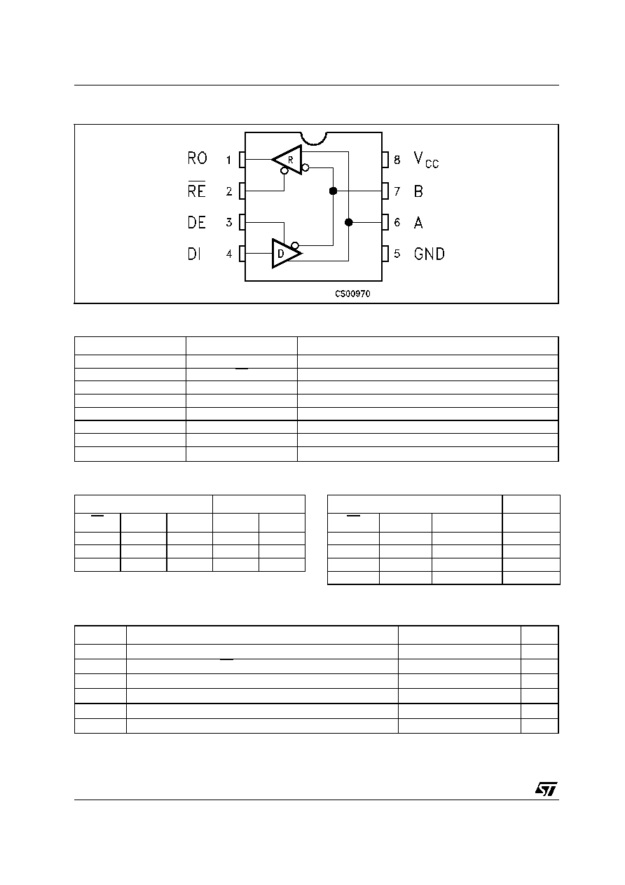
PIN CONFIGURATION
PIN DESCRIPTION
TRUTH TABLE (DRIVER)
X= Don't Care; Z=High Impedance
TRUTH TABLE (RECEIVER)
X= Don't Care; Z=High Impedance
ABSOLUTE MAXIMUM RATINGS
Absolute Maximum Ratings are those values beyond which damage to the device may occur. Functional operation under these condition is
not implied.
PlN N∞
SYMBOL
NAME AND FUNCTION
1
RO
Receiver Output
2
RE
Receiver Output Enable
3
DE
Driver Output Enable
4
DI
Driver Input
5
GND
Ground
6
A
Non-inverting Receiver Input and Non-inverting Driver Output
7
B
Inverting Receiver Input and Inverting Driver Output
8
V
CC
Supply Voltage
INPUTS
OUTPUTS
RE
DE
DI
B
A
X
H
H
L
H
X
H
L
H
L
X
L
X
Z
Z
INPUTS
OUTPUT
RE
DE
A-B
RO
L
L
+0.2V
H
L
L
-0.2V
L
L
L
INPUTS OPEN
H
H
L
X
Z
Symbol
Parameter
Value
Unit
V
CC
Supply Voltage
7
V
V
I
Control Input Voltage (RE, DE)
-0.5 to (V
CC
+ 0.5)
V
V
DI
Driver Input Voltage (DI)
-0.5 to (V
CC
+ 0.5)
V
V
DO
Driver Output Voltage (A, B)
±
14
V
V
RI
Receiver Input Voltage (A, B)
±
14
V
V
RO
Receiver Output Voltage (RO)
-0.5 to (V
CC
+ 0.5)
V

ST485E
3/13
ESD PERFORMANCE: TRANSMITTER OUTPUTS, RECEIVER INPUTS
DC ELECTRICAL CHARACTERISTICS
(V
CC
= 5V
±
5%, T
A
= T
MIN
to T
MAX
, unless otherwise specified. Typical values are referred to T
A
= 25∞C)
(See Note 1)
Note 1: All currents into device pins are positive; all cuttents out of device pins are negative; all voltages are referenced to device ground
unless specified.
Note 2: Supply current specification is valid for loaded transmitters when V
DE
= 0V
Note 3: Applies to peak current. See typical Operating Characteristics.
Symbol
Parameter
Test Conditions
Min.
Typ.
Max.
Unit
ESD
ESD Protection Voltage
Human Body Model
±
15
KV
ESD
ESD Protection Voltage
IEC-1000-4-2
±
8
KV
Symbol
Parameter
Test Conditions
Min.
Typ.
Max.
Unit
V
OD1
Differential Driver Output
(No Load)
5
V
V
OD2
Differential Driver Output
(With Load)
R
L
= 27
(RS-485) (See Fig. 1)
R
L
= 50
(RS-422) (See Fig. 1)
1.5
5
5
V
V
V
OD
Change in Magnitude of
Driver Differential Output
Voltage for Complementary
Output States
R
L
= 27
or 50
(See Fig. 1)
0.2
V
V
OC
Driver Common-Mode
Output Voltage
R
L
= 27
or 50
(See Fig. 1)
3
V
V
OC
Change in Magnitude of
Driver Common-Mode
Output Voltage for
Complementary Output
States
R
L
= 27
or 50
(See Fig. 1)
0.2
V
V
IH
Input High Voltage
RE, DE, DI
2.0
V
V
IL
Input Low Voltage
RE, DE, DI
0.8
V
I
IN1
Input Current
RE, DE, DI
±
2
µ
A
I
IN2
Input Current (A, B)
V
CM
= 0V or 5.25V
V
DE
= 0V
V
IN
= 12V
V
IN
= -7V
1
-0.8
mA
mA
V
TH
Receiver Differential
Threshold Voltage
V
CM
= -7 to 12V
-0.2
0.2
V
V
TH
Receiver Input Hysteresis
V
CM
= 0V
70
mV
V
OH
Receiver Output High
Voltage
I
O
= -4mA
V
ID
= 200mV
3.5
V
V
OL
Receiver Output Low
Voltage
I
O
= 4mA
V
ID
= -200mV
0.4
V
I
OZR
3-State (High Impedance)
Output Current at Receiver
V
O
= 0.4 to 2.4V
±
1
µ
A
R
IN
Receiver Input Resistance
V
CM
= -7 to 12V
24
K
I
CC
No Load Supply Current
(Note 2)
V
RE
= 0V or V
CC
V
DE
= V
CC
V
DE
= 0V
400
300
900
500
µ
A
µ
A
I
OSD1
Driver Short-Circuit Current,
V
O
=High
V
O
= -7 to 12V (Note 3)
35
250
mA
I
OSD2
Driver Short-Circuit Current,
V
O
=Low
V
O
= -7 to 12V (Note 3)
35
250
mA
I
OSR
Receiver Short-Circuit
Current
V
O
= 0V to V
CC
7
95
mA
ST485E
4/13
DRIVER SWITCHING CHARACTERISTICS
(V
CC
= 5V
±
5%, T
A
= T
MIN
to T
MAX
, unless otherwise specified. Typical values are referred to T
A
= 25∞C)
(See Note 1)
Note 1: All currents into device pins are positive; all cuttents out of device pins are negative; all voltages are referenced to device ground
unless specified.
RECEIVER SWITCHING CHARACTERISTICS
(V
CC
= 5V
±
5%, T
A
= T
MIN
to T
MAX
, unless otherwise specified. Typical values are referred to T
A
= 25∞C)
(See Note 1)
Note 1: All currents into device pins are positive; all cuttents out of device pins are negative; all voltages are referenced to device ground
unless specified.
Symbol
Parameter
Test Conditions
Min.
Typ.
Max.
Unit
t
PLH
t
PHL
Propagation Delay Input to
Output
R
DIFF
= 54
C
L1
= C
L2
= 100pF
(See Fig. 3 and 5)
25
45
ns
t
SK
Output Skew to Output
R
DIFF
= 54
C
L1
= C
L2
= 100pF
(See Fig. 3 and 5)
2
5
ns
t
TLH
t
THL
Rise or Fall Time
R
DIFF
= 54
C
L1
= C
L2
= 100pF
(See Fig. 3 and 5)
15
40
ns
t
PZH
Output Enable Time
C
L
= 100pF
S2 = Closed
(See Fig. 4 and 6)
35
50
ns
t
PZL
Output Enable Time
C
L
= 100pF
S1 = Closed
(See Fig. 4 and 6)
25
40
ns
t
PLZ
Output Disable Time
C
L
= 15pF
S1 = Closed
(See Fig. 4 and 6)
25
40
ns
t
PHZ
Output Disable Time
C
L
= 15pF
S2 = Closed
(See Fig. 4 and 6)
35
50
ns
Symbol
Parameter
Test Conditions
Min.
Typ.
Max.
Unit
t
PLH
t
PHL
Propagation Delay Input to
Output
R
DIFF
= 54
C
L1
= C
L2
= 100pF
(See Fig. 3 and 7)
110
130
ns
t
SKD
Differential Receiver Skew
R
DIFF
= 54
C
L1
= C
L2
= 100pF
(See Fig. 3 and 7)
5
10
ns
t
PZH
Output Enable Time
C
RL
= 15pF
S2 = Closed
(See Fig. 2 and 8)
11
35
ns
t
PZL
Output Enable Time
C
RL
= 15pF
S1 = Closed
(See Fig. 2 and 8)
13
35
ns
t
PLZ
Output Disable Time
C
RL
= 15pF
S1 = Closed
(See Fig. 2 and 8)
13
35
ns
t
PHZ
Output Disable Time
C
RL
= 15pF
S2 = Closed
(See Fig. 2 and 8)
11
35
ns
f
MAX
Maximum Data Rate
5
Mbps
ST485E
5/13
TEST CIRCUITS AND TYPICAL CHARACTERISTICS
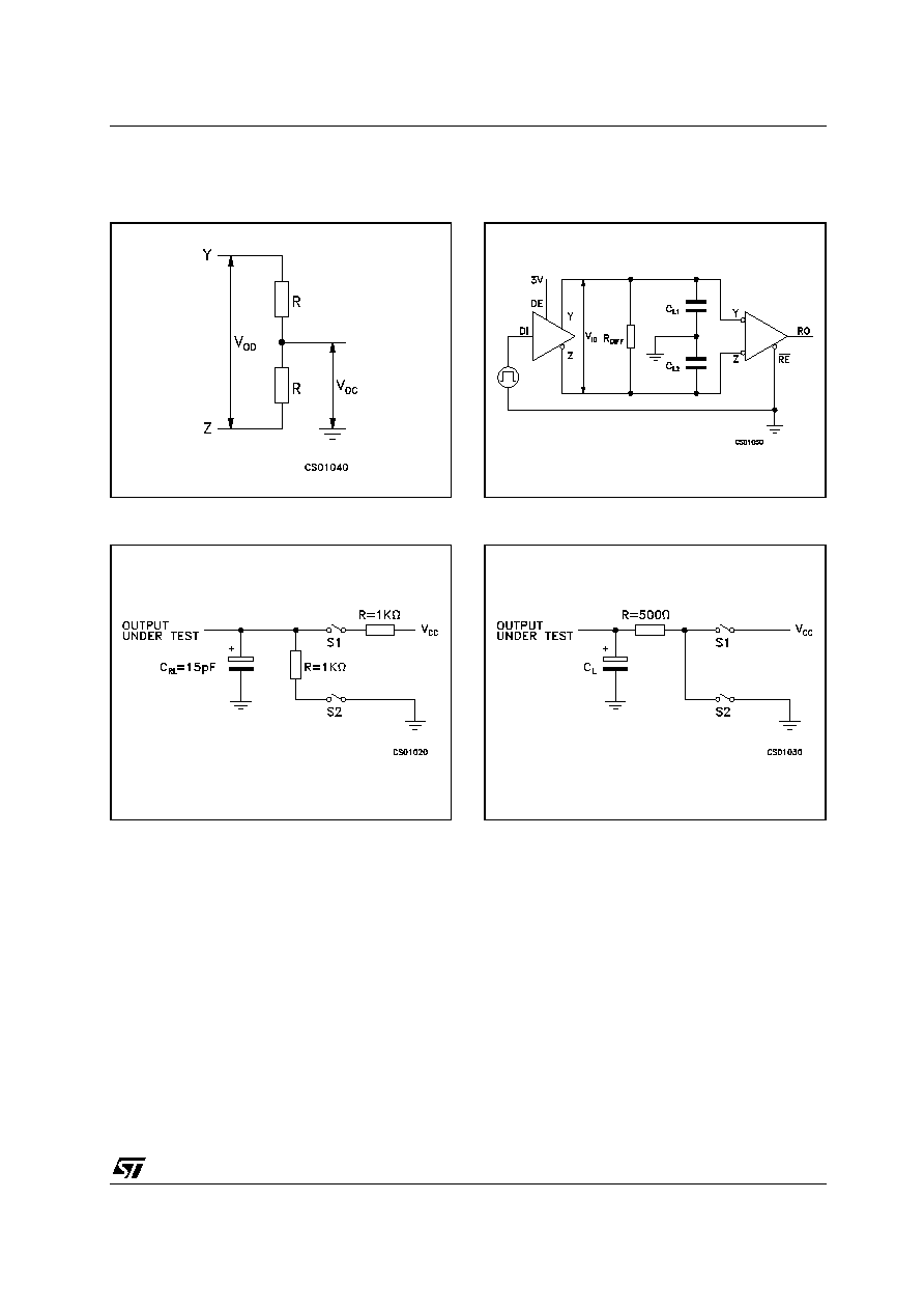
Figure 1 : Driver DC Test Load
Figure 2 : Receiver Timing Test Load
Figure 3 : Drive/Receiver Timing Test Circuit
Figure 4 : Driver Timing Test Load